Nut_stm32f103c8 Side-Channel Analysis
STM32F103C8 is a microcontroller chip based on the ARM Cortex-M3 core, launched by STMicroelectronics. Due to its high performance, low power consumption, and rich peripheral resources, this chip is widely used in embedded systems.
The Nut_stm32f103c8 development board is designed based on the STM32F103C8 chip and is suitable for side-channel analysis research and teaching of embedded chip firmware. This article uses Nut_stm32f103c8 as an example to demonstrate how to analyze power leakage of cryptographic algorithms using Cracker-S1.
Introduction to STM32F103
Main Specifications
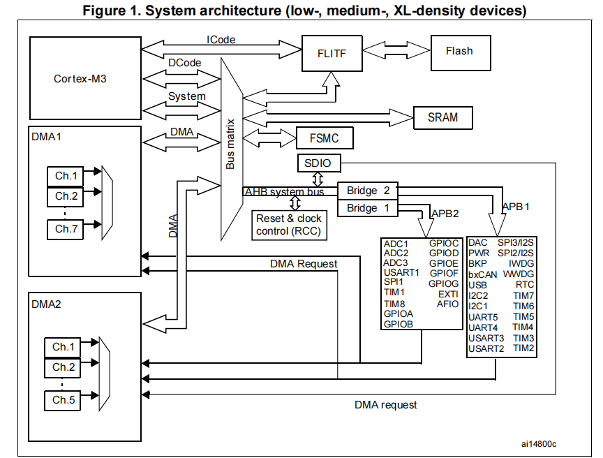
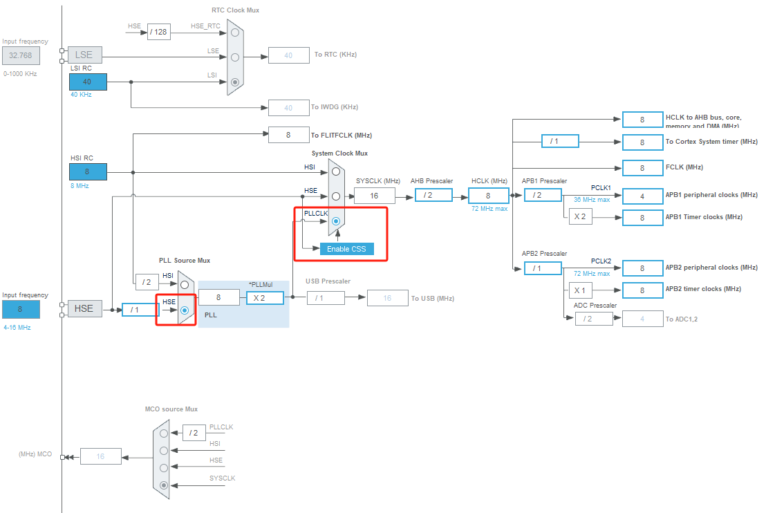
The architecture of the STM32F103C8 chip is shown below (RM0008).
Main specifications:
- Core: ARM 32-bit Cortex-M3 processor, up to 72MHz frequency, with single-cycle multiplication and hardware division.
- Memory:
- Up to 512KB Flash memory for program storage.
- Up to 64KB SRAM for data storage.
- Clock system:
- Internal 8MHz RC oscillator.
- Supports external 4-16MHz crystal.
- Clock multiplication via PLL.
- Peripherals:
- Up to 3 SPI interfaces, 2 I2C interfaces, 5 UART interfaces, 2 USB interfaces (one full-speed).
- Up to 18 timers including basic, general-purpose, and advanced timers.
- 12-bit ADC with up to 16 channels.
- 12-bit DAC with up to 2 channels.
- CAN interface (on some models).
- Operating voltage: 2.0V to 3.6V.
- Package types: LQFP, LFBGA, UFQFPN, WLCSP, etc., providing various pin counts for different design needs.
- Low power modes: Sleep, Stop, and Standby modes to reduce power consumption, suitable for battery-powered applications.
- Development support: ST provides comprehensive software tools, including STM32CubeMX configuration and HAL libraries, facilitating programming and debugging.
The STM32F103 series is widely applied in industrial control, consumer electronics, smart home, IoT, and other fields due to its cost-effectiveness, ease of development, and strong community support.
Clock System
STM32F103 clocks can be divided into internal clocks and external clocks:
-
Internal Clocks (HSI/LSI):
-
Advantages: No external components needed, low cost, fast startup, strong interference resistance.
-
Disadvantages: Low accuracy (RC oscillator), suitable for non-critical scenarios (e.g., watchdog, emergency backup).
-
-
External Clocks (HSE/LSE):
-
Advantages: High accuracy (crystal oscillator), stable, suitable for high-speed communication and real-time timing (e.g., USB, RTC).
-
Disadvantages: Requires external crystal, increases hardware cost, slightly longer startup time.
-
Side-Channel Analysis Comparison under Different Clock Configurations and Sampling Rates
HSI + 48M Samples/S Asynchronous Sampling
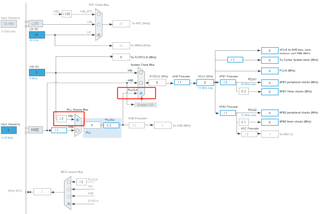
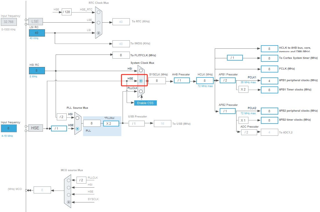
The chip system clock uses internal HSI clock source, SYSCLK configured to 8MHz, sampling rate set to 48M Samples/S (an integer multiple of SYSCLK), internal clock configuration shown below.
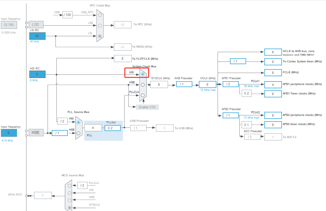
The clock source is internal 8MHz HSI RC, through System Clock Mux, resulting in SYSCLK at 8MHz.
Understanding HSI, HSE, PLL clock configurations is necessary, as side-channel signal acquisition and power analysis results vary greatly under different clock modes.
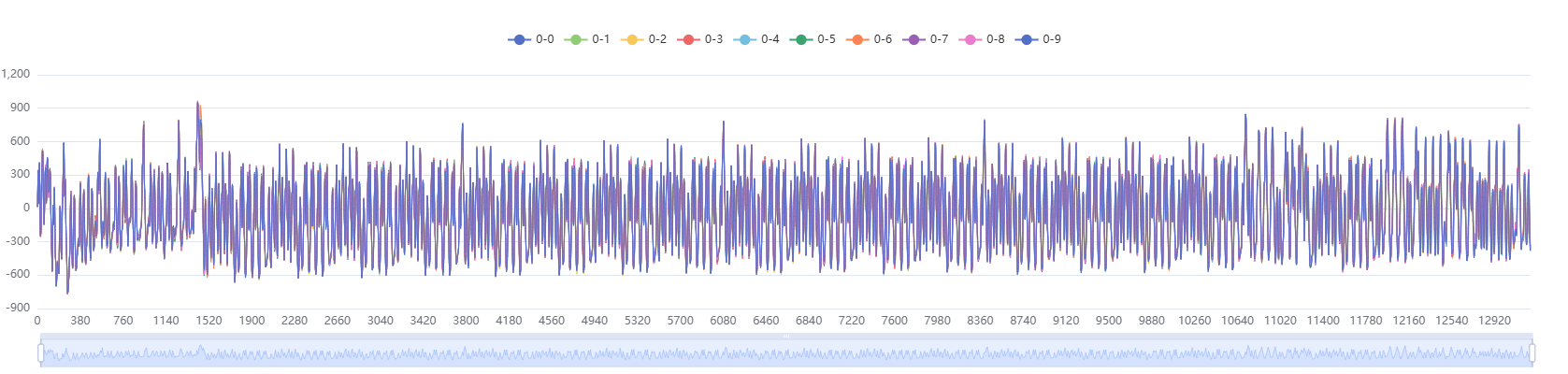
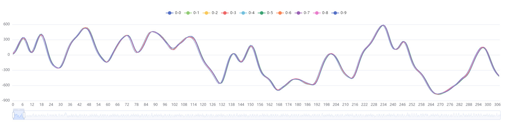
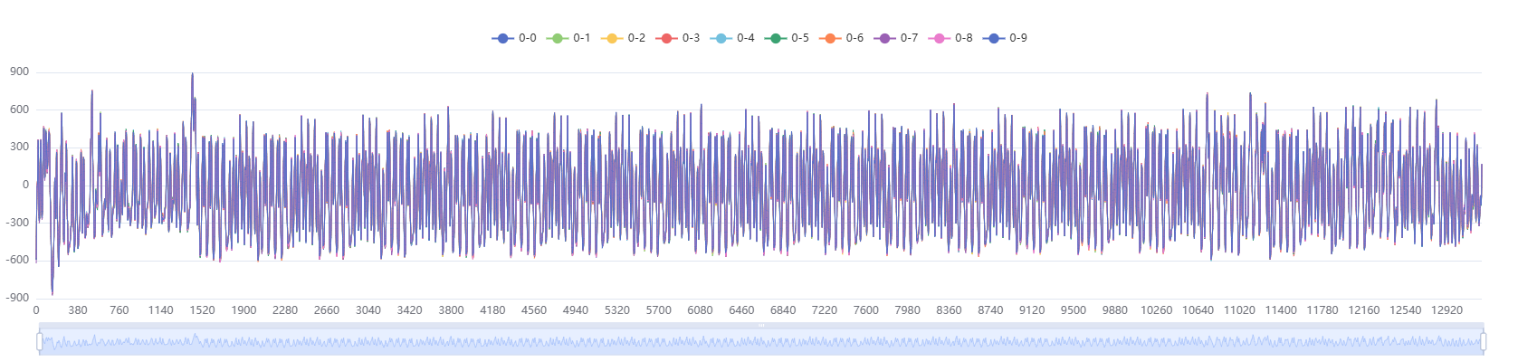
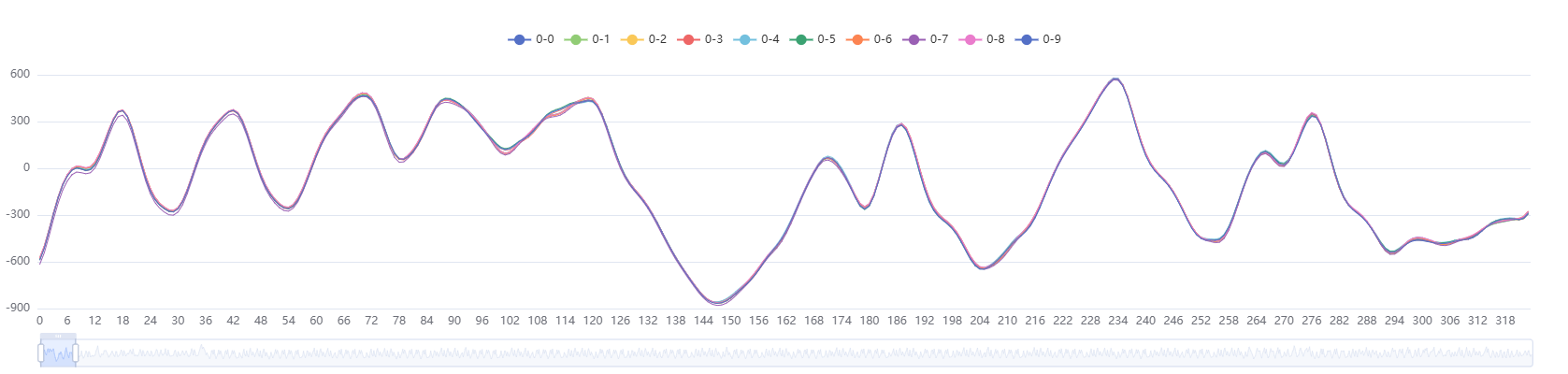
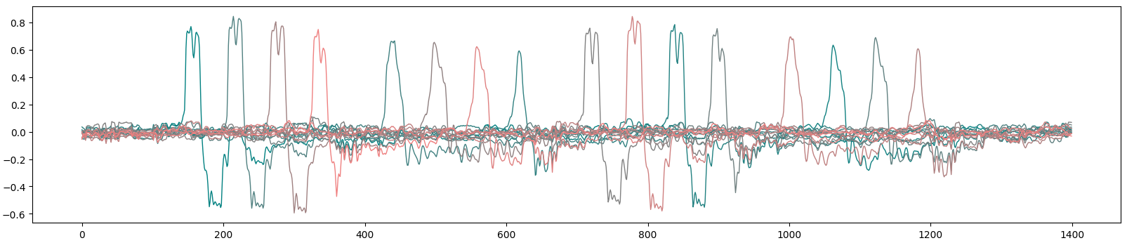
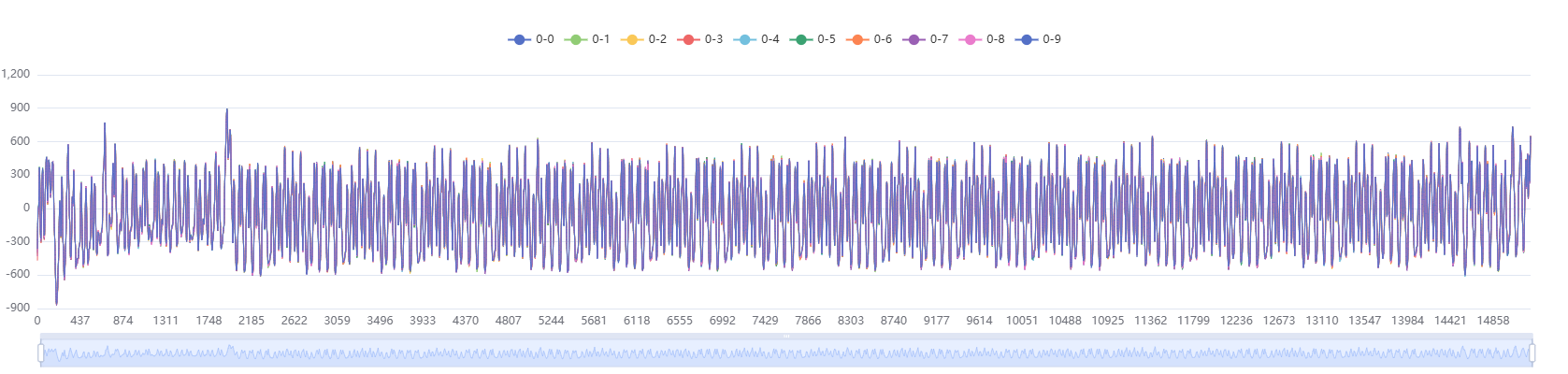
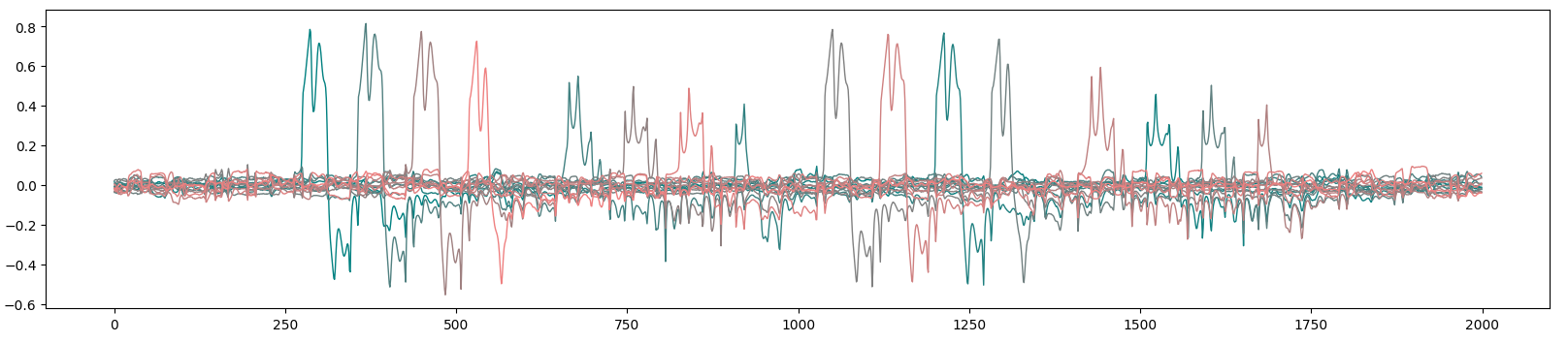
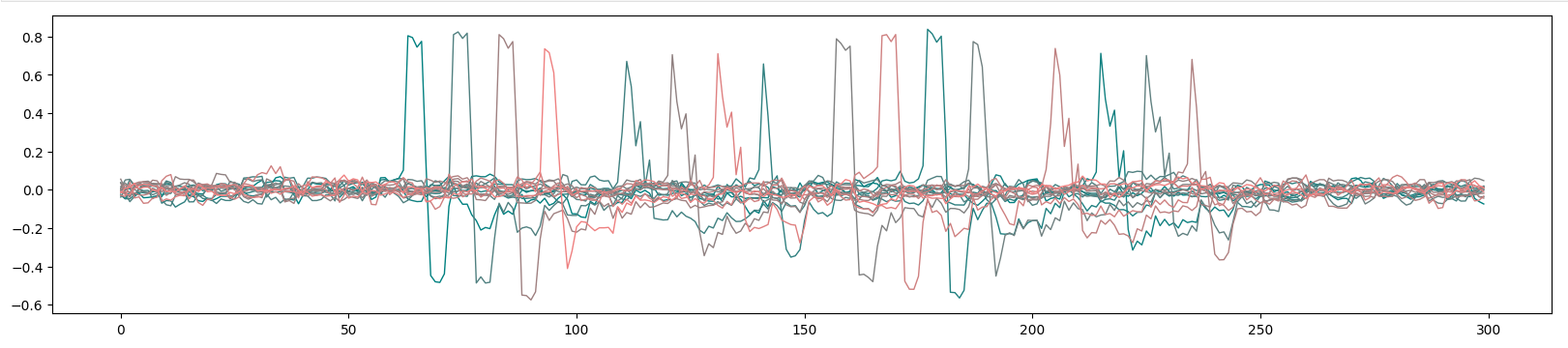
The AES software implementation power traces collected are shown below, displaying the first 10 traces, clearly showing the features of 16 rounds encryption.
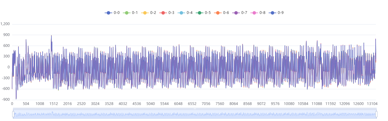
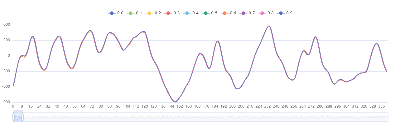
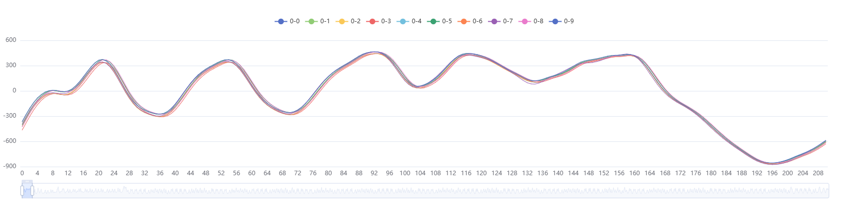
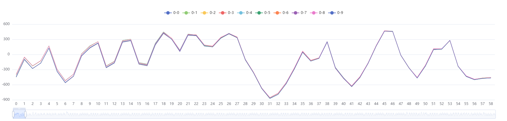
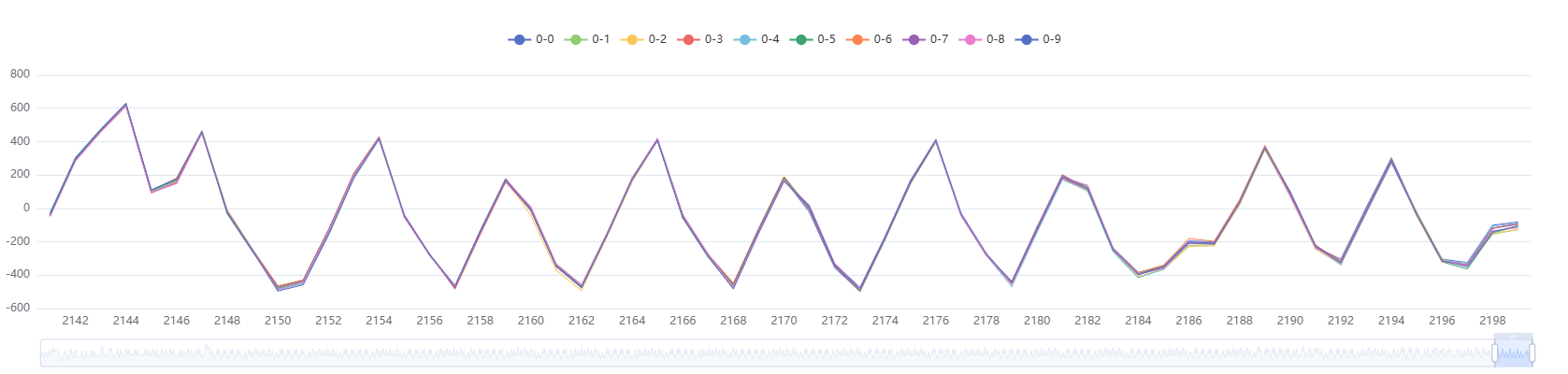
Zooming in on the beginning of the traces shows good overlap.
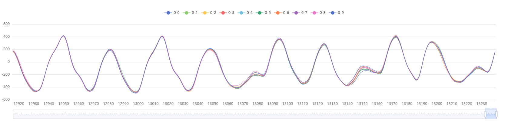
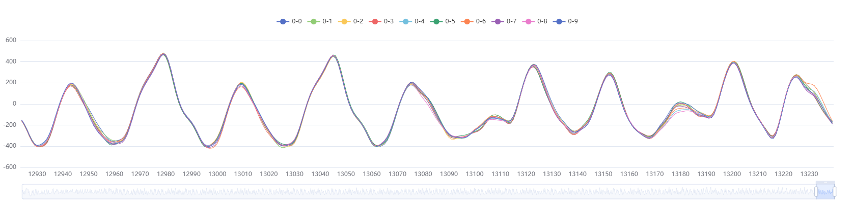
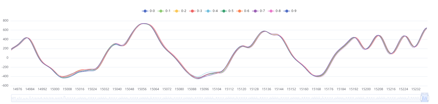
Zooming in on the end shows reduced overlap.
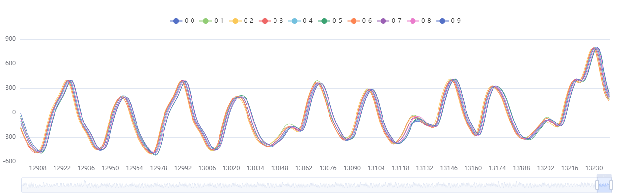
The clock generated by internal high-speed clock HSI is unstable, causing poor time alignment of the traces.
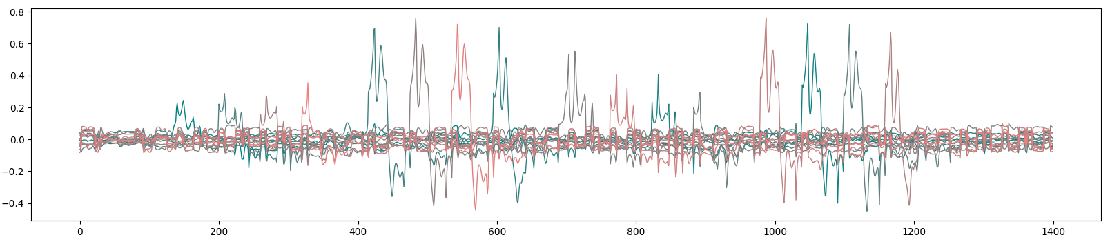
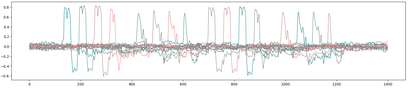
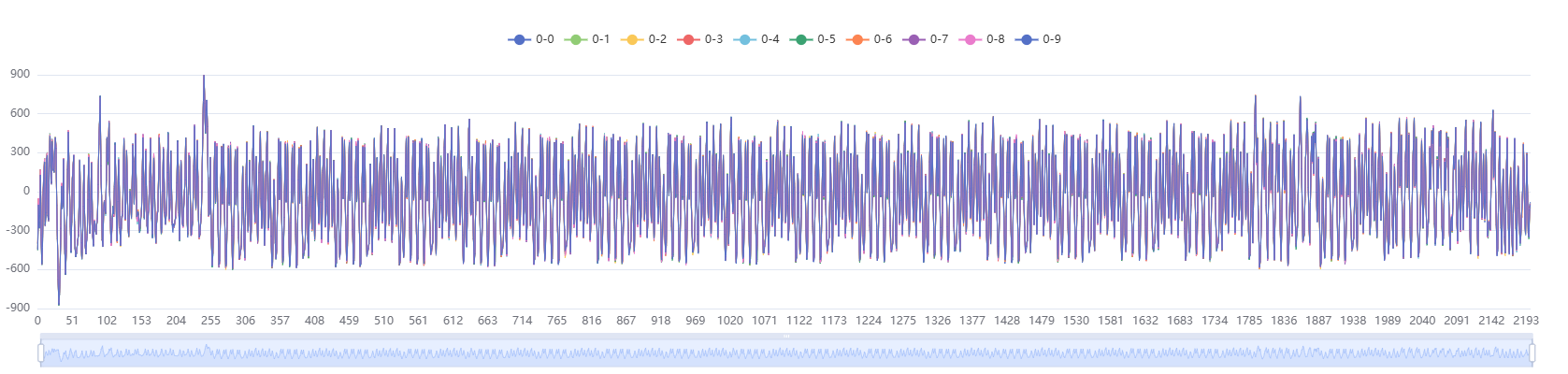
CPA analysis on the first round S-box output of 1000 traces is shown below.
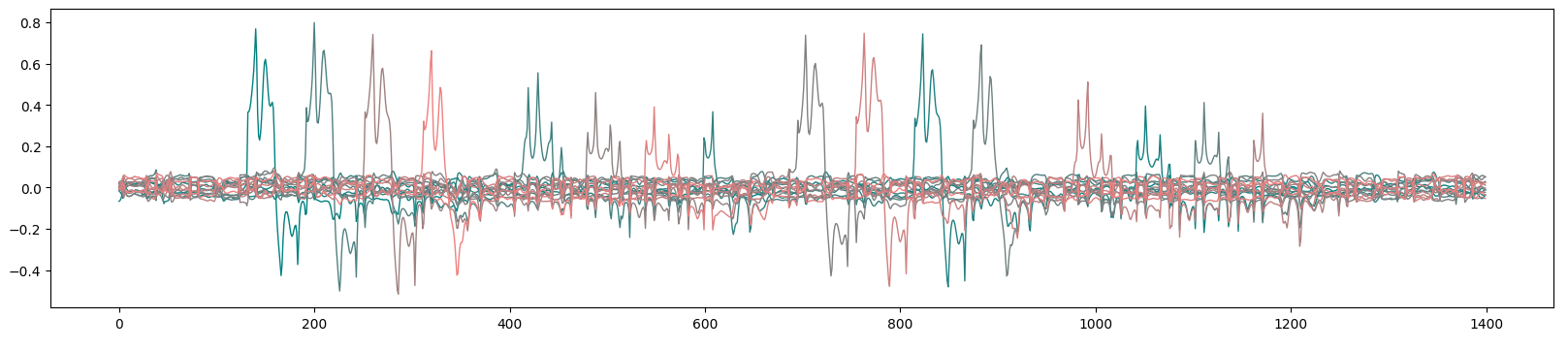
Two key usage patterns appear, with maximum correlation close to 0.8 indicating key leakage.
HSI + PLL + 48M Samples/S Asynchronous Sampling
The chip system clock uses internal HSI + PLL clock source, SYSCLK configured to 8MHz, sampling rate set to 48M Samples/S (an integer multiple of SYSCLK), internal clock configuration shown below.
AES power traces collected, showing the first 10 traces, clearly showing 16 rounds encryption.
Zooming in on the beginning shows good overlap.
Zooming in on the end shows reduced overlap.
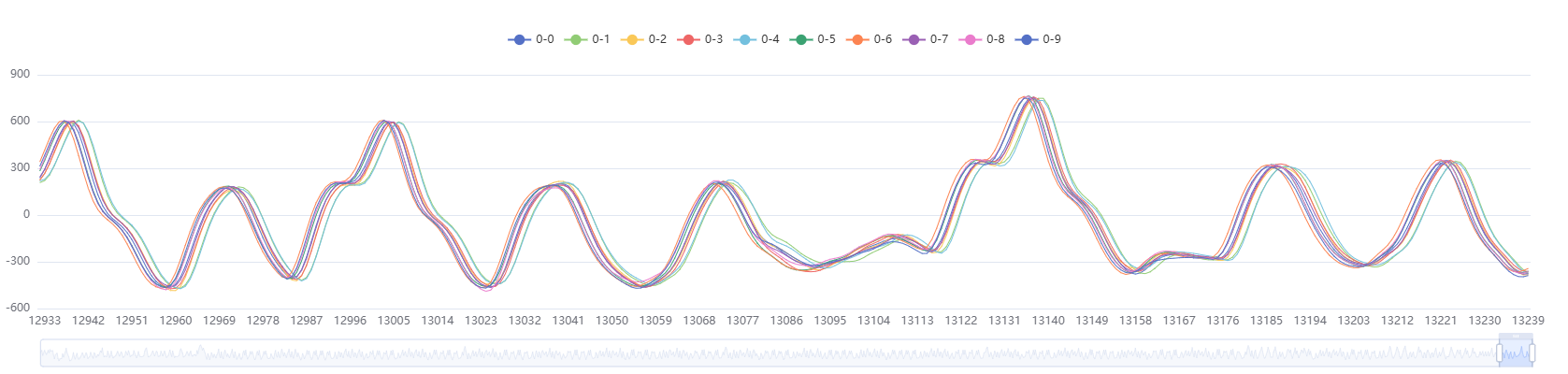
Clock generated by internal HSI with PLL is unstable, causing poor time alignment of traces.
CPA analysis on the first round S-box output of 1000 traces is shown below.
Two key usage patterns appear, maximum correlation close to 0.8. Compared to HSI only mode, every 4-byte leakage patterns differ significantly.
HSE + 48M Samples/S Synchronous Sampling
The chip system clock uses external HSE clock source, SYSCLK configured to 8MHz, sampling rate set to 48M Samples/S (an integer multiple of SYSCLK), clock configuration shown below.
When using HSE external clock, enable Cracker-S1 external clock output.

AES power traces collected, showing the first 10 traces, clearly showing 16 rounds encryption.
Zooming in on the beginning shows good overlap.
Zooming in on the end shows no loss of overlap.
CPA analysis on the first round S-box output of 1000 traces is shown below.
Two key usage patterns appear, maximum correlation exceeding 0.8. Compared to both HSI modes, leakage is significantly stronger.
STM32 external clock and ADC sampling clock share the same source, ensuring precise acquisition of 6 data points per cycle (48M/8M), greatly improving side-channel analysis success rate.
HSE + PLL + 48M Samples/S Synchronous Sampling
The chip system clock uses internal HSE + PLL clock source, SYSCLK configured to 8MHz, sampling rate set to 48M Samples/S (an integer multiple of SYSCLK), internal clock configuration shown below.
When using HSE external clock, enable Cracker-S1 external clock output.
AES power traces collected, showing the first 10 traces, clearly showing 16 rounds encryption.
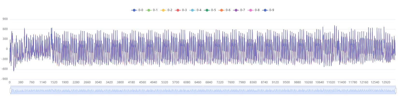
Zooming in on the beginning shows good overlap.
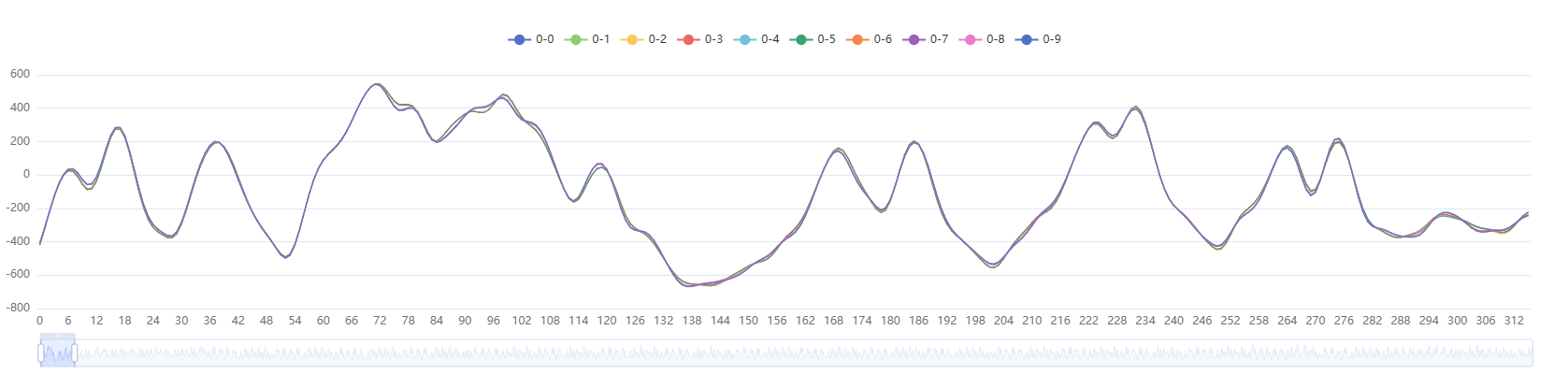
Zooming in on the end shows good overlap.
CPA analysis on the first round S-box output of 1000 traces is shown below.
Two key usage patterns appear, maximum correlation exceeding 0.8. Compared to both HSI modes, leakage is significantly stronger.
HSE + 65M Samples/S Asynchronous Sampling
This test uses external 8MHz clock, sampling rate increased to 65M Samples/S, sampling rate increased but not an integer multiple of clock frequency.
AES power traces collected, showing the first 10 traces, clearly showing 16 rounds encryption.
Zooming in on the beginning shows worse overlap.
Zooming in on the end shows worse overlap.
CPA analysis on the first round S-box output of 1000 traces is shown below.
Two key usage patterns appear, maximum correlation exceeding 0.8. Compared to synchronous sampling, although sampling rate increased, key correlation decreased.
HSE + 8M Samples/S Asynchronous Sampling
This test uses external 8MHz clock, sampling rate reduced to 8M Samples/S, sampling rate decreased and equal to chip clock frequency.
AES power traces collected, showing the first 10 traces, clearly showing 16 rounds encryption.
Zooming in on the beginning shows good overlap.
Zooming in on the end shows good overlap.
CPA analysis on the first round S-box output of 1000 traces is shown below.
Two key usage patterns appear, maximum correlation exceeding 0.8.
Comparison of Side-Channel Analysis Effects under Different Modes
| Mode | Analysis Result |
|---|---|
| HSI + 48M Async Sampling | |
| HSI + PLL + 48M Async Sampling | |
| HSE + 48M Sync Sampling | |
| HSE + PLL + 48M Sync Sampling | |
| HSE + 65M Async Sampling | |
| HSE + 8M Sync Sampling | |
Analysis results show that external clock + synchronous sampling performs best. To save computation time, using chip clock at the same frequency with synchronous sampling is also recommended.
Related scripts and data files can be downloaded at https://pan.baidu.com/s/1jLVV_ViPUspbqgIOSOFyOQ?pwd=utyy.